[Home] [Digital Signal Processing route] [Published Articles]
[Local QRM/noise reduction] [Very small vertical magnetic loop]
[Medium size vertical magnetic loop] [Vertical magnetic Alford loop]
[Vertical magnetic loops in real life] [Circular polarization]
[Broadband amplification] [Broadband amplifier] [Single chip amplifier]
[Dual loop antenna system] [Hints]
[Phaser 80 – 10 meters] [Balancing and closed loop antennas]
Broadband loop amplifier (update March 2022 of 2018 and of 2003 design)
The broadband loop amplifier design requirements
- Bandwidth starting from 1.8MHz or lower and up to 30MHz
- Noise contribution lower than the rural ambient noise level
- Best balancing and decoupling from the feeding coaxial cable (minimizing coupled man-made noise and for measurement applications)
- Very good large signal behavior (IM products <= noise level of the amplifier)
- Output level comparable to the half wave dipole
- Controlled gain (especially if using loops in matched pairs and for measurement applications)
- Overload protected (your own transmit signal e.g.)
- Receiver maximum input level limited to about 13dBm
- Filtering potentially overloading local out of band (VHF) signals
- Using regular components, not too complex circuit, no SMD’s (junk box)
- Low visibility of the loop for neighbors
Of course the result will be a compromise, on all aspects good enough.
(see for the principle of the amplification: Broadband amplification)
Design and specification bandwidth: 1MHz-30MHz
Note: balancing and visibility both are very relevant on a residential location. Especially balancing is most relevant because of the high man-made noise levels on residential locations.
Practical implementation of the active broadband loop amplifier
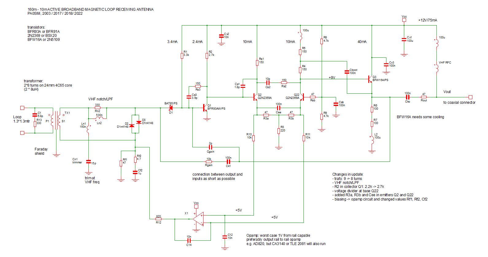
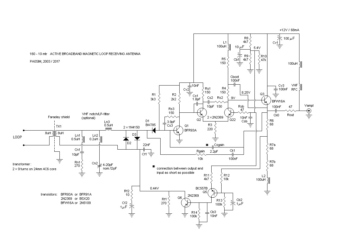
This is a 2022 update of the 2018 and the 2003 design (2003 version).
Note: matching circuit diagram for the PCB is in: Broadband_active_loop_PA0SIM.pdf
The demo version of Simetrix is preferred for design and simulation instead of PSPICE. It is much more intuitive and aimed at the design process. Results match measurements.
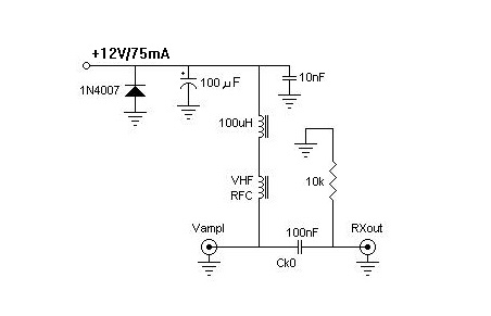
This trans-impedance amplifier is not very complex. The amplifier consists of three stages. The transistor Q1 is optimized for noise in a Common Emitter (CE) circuit. The output stage Q3 has to deliver the power to the load. The intermediate stage Q2 and Q22 provides extra amplification to get the desired large signal behavior.
The gain (antenna factor) is set with Rgain and Csgain. Csgain is used to stabilize the amplifier.
The opamp X1 controls the DC bias levels. The response is fast enough to recover from an overload when doing QSK. Remember that your own transmit signal easily overloads the amplifier. Worst case the output of the opamp has to be 1Volt from rail capable.
The diodes D1, D2 and D3 protect the amplifiers input stage (also from your own transmit signal).
The VHF-notch/low pass filter attenuates strong local VHF transmitters.
The transformer together with the Faraday shield take care of the balancing and the common mode suppression. The coupling factor k of the transformer is 0.8. Inductances are 8uH.
The resistor R13 and capacitor C1 at the input compensate for the 0.8 coupling factor for frequencies >14MHz. They are only usable in combination with this transformer design.
The design assumes a 1.3m*1.3m loop with 2-3mm diameter wire. The impedance of the loop is also relevant for the large signal behavior via the amplifiers loop gain.
With a 1.3m*1.3m loop with 2mm diameter wire the antenna factor (E/Vo) is about 0.5.
Expected Antenna Factor
In the next plot the transmission line circuit model of the loop is used.
Simulation behavior model of the loop will be less accurate for frequencies >14MHz.
Note: measured gain 1MHz-30MHz of the amplifier is according simulation within 1dB.

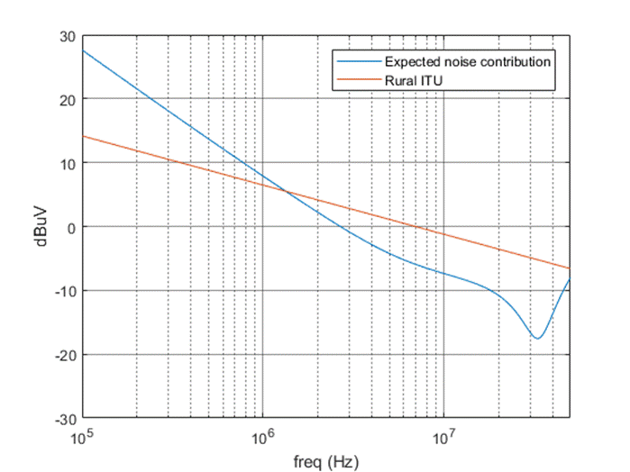
Expected noise contribution
Measured output noise of the amplifier is according simulation within 1-2dB.
Noise contribution is 5-6dB lower than ITU rural noise level. As far as the used antenna behavioral model is accurate.
Measured noise increase at a better than rural location: 4dB.
Large signal behavior
IM3 >+40dB and IM2>+70dB for frequencies <10MHz
The following plot shows the measured results in the (version 2003) simulation (PSPICE).
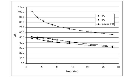
The large signal behavior measured in simulation (PSPICE).
Measurements indicate a better large signal behavior. E.g. the second harmonic at 14MHz of a 7MHz S9+60dB signal is clearly lower than 39dB below S9. That is more than 105dB below the 7MHz amplitude. On 14MHz it can just be heard deep in the noise without the loop connected and so with only the noise of the amplifier.
Common mode rejection and Faraday shield
Measured common mode rejection > 50dB without Faraday shield.
Rejection is measured as voltage difference between the loop and the amplifier ground to output voltage. With the loop at ground level and amplifier ground connected to ground, this voltage difference is about equal to the electrical field E.
An E-shaped Faraday shield can be applied at the transformer improving common mode rejection by another 6-10dB. Shield soldered to ground only at the outer legs.
Routing the coaxial cable
The coaxial cable can and will pick up noise in the shack. It will act as an antenna and reradiate this noise. The resulting electromagnetic field can be pick up by the loop.
There are several ways to minimizing receiving this noise by the loop:
- keep the coaxial cable perpendicular to the loop, preferably straight down
- run the coaxial cable underground to the shack
- add current baluns /ferrite (not preferred, work around)
Bias-T power supply (needs low series resistance 100uH inductors!)
Amplifier PCB with Faraday shield
PCB design by PA3CSG.
The PCB is available through the Maasbree WebSDR website.
This amplifier is now used for the Maasbree WebSDR.
More information with matching circuit diagram, is in Broadband_active_loop_PA0SIM.pdf

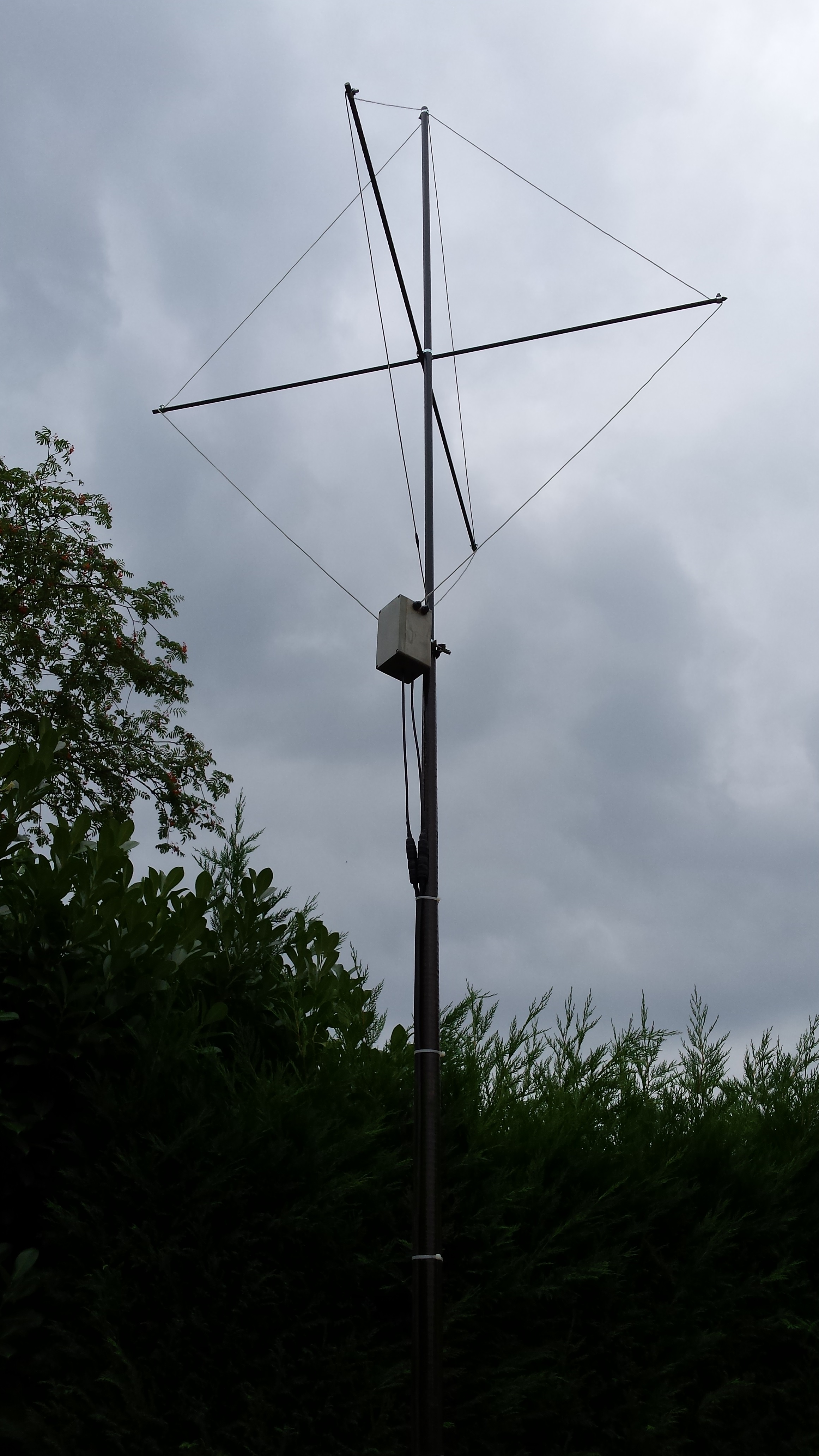
Two orthogonal loops
Discussion on the main design compromises
- Noise contribution lower than the ambient rural noise level
Using the common emitter (CE) circuit for Q1 for best noise behavior with the emitter directly to ground for minimal inductance, increases the complexity of the DC biasing.
- Best balancing and decoupling from the feeding coaxial cable
The chosen transformer coupling is the easiest and most controlled way of maximizing the balancing. However the coupling factor k is 0.8. This attenuates the signal amplitude about 2-3dB and increases the noise contribution of the amplifier with 2-3dB. It also affects the flatness of the antenna factor, but at the same time it enables a better noise behavior at around 30MHz. The turn ratio 1:1 is also a compromise. Optimal noise impedance matching is not possible over the full 1MHz-30MHz bandwidth.
- Using regular components, not too complex circuit, no SMD’s
Only the BFR93A is SMT
- Low visibility for neighbors
Limiting the diameter of the loop wire to 2-3mm increases the noise contribution of the amplifier with <3dB, but improves large signal behavior.
Last update: June 15, 2023
© PA0SIM